Trends
Sci.
2026;
23(8):
12946
Effect of Gold-Modified Titanium Dioxide Thin Films on Electrical Resistance, Optical Transmittance, and Wetting Properties
Phinkaew Maisungnoen and Buppachat Toboonsung*
Faculty of Science and Technology, Nakhon Ratchasima Rajabhat University, Nakhon Ratchasima 30000, Thailand
(*Corresponding author’s e-mail: [email protected])
Received: 8 December 2025, Revised: 24 December 2025, Accepted: 31 December 2025, Published: 10 March 2026
Abstract
Titanium dioxide (TiO2) thin films were synthesized via the sparking process at different durations and modified with gold (Au) by DC magnetron sputtering to study the effects of microstructure, plasmonic interactions, and interfacial charge transport. Pristine TiO2 films showed a transition from fine, uniform nanograins (1 h) to agglomerated structures (3 - 5 h), reducing transparency and increasing defect density, while thicker films exhibited improved electrical continuity. The 1 h TiO2 film offered the optimal balance of high transparency (~90%), uniform morphology, and long-term hydrophilicity. Au deposition significantly influenced film properties: Increasing sputtering current (10 - 50 mA) enhanced Au loading, transforming discontinuous nanoparticles into a percolated network at 30 mA, and causing agglomeration at 50 mA. This morphology controlled plasmonic absorption, sub-band-gap optical behavior, and conductivity. Au modification reduced sheet resistance from 37 MΩ/sq to 5.8 Ω/sq (30 mA) and enabled visible-light absorption via localized surface plasmon resonance and metal-induced gap states. Au-coated films maintained water contact angles <30° over 60 days, attributed to stabilized surface hydroxylation and suppression of hydrocarbon adsorption. Sputtering at 30 mA produced the optimal Au-TiO2 architecture, balancing transparency, conductivity, plasmonic activity, and durable wettability, offering a promising approach for low-cost transparent coatings, optoelectronic devices, and self-cleaning surfaces.
Keywords: Titanium dioxide, Gold, Thin films, Sparking process, Sputtering deposition, Four-point probe, Sheet resistance, Hydrophilicity stability
Introduction
Titanium dioxide (TiO2) thin films remain one of the most widely studied oxide materials because of their high transparency [1,2], chemical stability [3], photocatalytic activity [3], and compatibility with various substrates [4]. These attributes enable the use of TiO2 films in diverse applications, including optical and protective coatings [5], environmental monitoring devices [6,7], and surface technologies [8,9] that rely on controlled wettability and surface energy. As the demand for low-cost and scalable thin-film fabrication methods continues to increase, the sparking process has gained renewed interest. This method enables the direct production of clean TiO2 nanoparticles and thin films on substrates, eliminating the need for chemical precursors, surfactants, or high-temperature processing, making it
an attractive option for rapid and environmentally friendly material deposition [10,11]. Although TiO2 possesses many useful characteristics, several limitations still hinder its broader use in advanced optical and electronic devices. It is a wide band gap that restricts absorption to the ultraviolet region [12,13], the intrinsic electrical conductivity is relatively low [14,15], and the well-known aging effect can cause hydrophilic surfaces to gradually revert to a more hydrophobic state through hydrocarbon adsorption [16-18]. In recent years, noble-metal modification, particularly with gold (Au), has been explored to address these shortcomings. Au nanoparticles have been shown to interact with TiO2 through multiple mechanisms: Improving charge transfer efficiency, enhancing visible-light absorption via localized surface plasmon resonance (LSPR), and stabilizing surface wettability by suppressing surface contamination. These plasmonic and electronic interactions can significantly alter the functional properties of TiO2 thin films [19-23].
Current literature indicates that the influence of Au on TiO2 is highly sensitive to how Au is incorporated. Parameters such as Au loading amount, particle distribution, nanoparticle size, and clustering behavior strongly determine the resulting optical transmittance, band-gap behavior, charge-transport characteristics, and surface chemistry of the composite film [19-25]. These effects are particularly relevant for sputtering techniques, in which the sputtering current plays a key role in defining particle density and surface coverage [19,21,24]. Higher sputtering currents generally lead to greater Au deposition but can also promote aggregation, which may either enhance or hinder electron transport and optical transparency [24,25]. Thus, understanding the interplay between sputtering parameters and film performance is crucial for optimizing Au-modified TiO2 thin films [12,21]. While numerous studies have examined Au-TiO2 nanostructures, most focus on powder-based systems or films produced using conventional deposition techniques [3,4,22]. Reports that combine the sparking process, a unique physical synthesis route, with controlled Au sputtering remain limited. Sparking-derived TiO2 films exhibit distinctive surface morphology and defect structures that differ from those produced by sol-gel or vacuum-based methods and therefore may respond differently to Au modification [5,10,11,13]. This gap highlights the need for systematic investigation on how Au deposition affects sparking-grown TiO2 thin films, particularly in terms of their optical, electrical, and surface-wetting behaviors [19,20,23].
In this study, TiO2 thin films were first fabricated using the sparking process at different durations to determine an optimal condition based on surface morphology, optical transparency, electrical resistance, and hydrophilicity performance [10,11]. The best-performing TiO2 film was then coated with Au using sputtering currents of 10, 30 and 50 mA to investigate how varying Au coverage influences the structural, optical, electrical, and wetting characteristics of the resulting films [19-21,24,25]. The findings provide insight into the combined effects of sparking and noble-metal sputtering on TiO2 thin films and offer useful guidelines for designing low-cost functional coatings for optical, electronic, and surface-engineering applications.
Materials and methods
Titanium dioxide (TiO2) thin films were deposited onto glass substrates (1×1 cm²) using the sparking technique. High-purity titanium wires (99.98%, 0.25 mm diameter, Advent Research Materials Ltd.) were assembled into 10 electrode pairs and subjected to a high voltage of 6 - 7 kV for sparking durations of 1, 3 and 5 h, following the procedures described in [10,11]. The gap between each pair of Ti-wire electrodes was maintained at approximately 1 - 2 mm, and all depositions were performed at room temperature. During sparking, titanium nanoparticles generated by the discharge were oxidized in ambient air and deposited uniformly onto the glass surface, forming TiO2 thin films of different thicknesses and surface morphologies depending on sparking time. The obtained TiO2 films were then characterized to determine the optimal deposition condition before gold coating. The surface morphology, crystal structure, optical transmittance, electrical resistance, and wettability of all TiO2 films were analyzed. Based on these results, the film fabricated at a sparking duration of 1 h was identified as the optimal sample, exhibiting the best balance between surface uniformity, high transparency, and stable hydrophilicity.
Subsequently, gold (Au) was deposited on the optimized TiO2 thin films using a DC magnetron sputtering system (Quorum Q150RS) to modify and enhance its optical and electrical properties. The sputtering process was conducted at currents of 10, 30 and 50 mA for 30 s under a controlled vacuum pressure of approximately 5×10⁻² mbar. The Au target was positioned at a distance of 75.50 mm from the TiO2 thin-film substrates. The structural, morphological, optical, electrical, and surface-wetting characteristics of the TiO2 and Au-TiO2 films were comprehensively investigated using various analytical techniques. The Au deposition rate was estimated based on the manufacturer-calibrated sputtering rate of the Quorum Q150RS system under fixed operating conditions. In situ thickness monitoring, such as a quartz crystal microbalance (QCM), was not employed; therefore, the reported Au thickness represents an equivalent nominal estimate. The surface morphology and elemental composition of the films were examined using scanning electron microscopy (SEM, JEOL JSM-6335F) equipped with energy-dispersive X-ray spectroscopy (EDS) to evaluate the compositional uniformity of the thin films. Cross-sectional SEM images were further used to determine the film thickness. The thickness of TiO2 thin films was measured from the glass-substrate interface to the top surface of the TiO2 layer along the cross-section, and the average value with standard deviation was reported. The crystalline phase was identified by Raman spectroscopy (SENTERRA II) with a 532 nm excitation laser operating at 12.5 mW, confirming the anatase phase of TiO2 and the successful incorporation of Au after sputtering. The optical transmittance was measured using ultraviolet-visible (UV-Vis) spectrophotometry (GENESYS 10S), and the optical band gap (Eg) was determined by Tauc plot analysis. The electrical properties were evaluated as the sheet resistance by the four-point probe method (JANDEL Model RM3-AR) at a constant current of 10 mA. The surface wettability was determined by measuring the static water contact angle with image analysis. The contact-angle measurements were performed immediately after film fabrication and at regular intervals for up to 60 days to assess long-term hydrophilicity. All characterizations were performed under ambient laboratory conditions, and each measurement was repeated at least five times to ensure data reliability. In addition, the film deposition experiments were independently repeated under identical conditions to confirm the reproducibility of the fabrication process.
Results and discussion
Morphology of TiO2 thin films
Figure 1 presents SEM micrographs of TiO2 thin films prepared at sparking durations of 1, 3 and 5 h, where images (Figures 1(a) - 1(c)) show the top-view morphology and images (Figures 1(d) - 1(f)) illustrate the corresponding cross-sectional structures. The surface morphology reveals the formation of granular nanoparticles uniformly distributed on the glass substrate. At a sparking time of 1 h (Figures 1(a) and 1(d)), the particles appear fine and well-dispersed, forming a relatively smooth and homogeneous surface. The corresponding cross-sectional thickness is 247 ± 70 nm, indicating the formation of a thin and uniformly deposited TiO2 layer. When the sparking duration increases to 3 h (Figures 1(b) and 1(e)), partial aggregation of TiO2 nanoparticles begins to occur, resulting in a rougher surface texture. This structural evolution is accompanied by a significant increase in film thickness to 571 ± 179 nm, suggesting enhanced grain growth and vertical accumulation of nanoparticles. At 5 h (Figures 1(c) and 1(f)), large clusters and dense agglomerates are observed, indicating excessive particle growth and coalescence due to prolonged sparking. The cross-sectional thickness further increases to 1,003 ± 386 nm, confirming that extended sparking time promotes continuous nanoparticle deposition and substantial film thickening, albeit with higher surface irregularity. It is noted that the increase in sparking time evidently promotes nucleation, grain growth, and agglomeration, leading to increased surface irregularity and thicker film formation. The 1 h sparking sample exhibits a fine-grained morphology with uniform nanostructure and the most consistent layer thickness, whereas longer sparking durations (3 - 5 h) result in irregular particle agglomeration and increased surface defects. Therefore, a sparking duration of 1 h is considered the optimal condition for achieving a uniformly coated TiO2 thin film with balanced surface coverage and controlled thickness. Moreover, the observed nanoparticle aggregation and porous morphology are consistent with sparking-derived TiO2 thin films reported in literature [26].
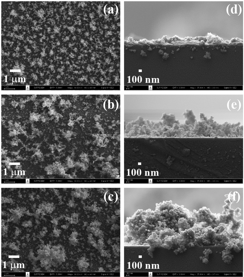
Figure 1 SEM images of TiO2 thin films prepared at sparking durations of 1, 3 and 5 h: (a) - (c) top-view morphology and (d) - (f) cross-sectional structures.
Raman analysis of TiO2 thin films
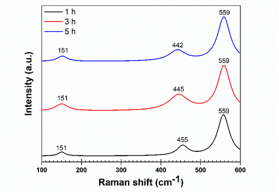
Figure 2 shows the Raman spectra of TiO2 thin films synthesized at sparking durations of 1, 3 and 5 h. All films exhibit 3 major vibrational modes centered at approximately 151, 445 - 455, and ~559 cm−1, which are characteristic of nanocrystalline anatase TiO2. The strongest band at ~151 cm−1 corresponds to the Eg mode. Its blue-shift and broadened FWHM relative to bulk anatase indicate the influence of phonon confinement, nanoscale crystallite domains, and lattice disorder, consistent with previous observations in nanocrystalline TiO2 systems [27-29]. The band at 445 - 455 cm−1, assigned to the B1g/Eg modes, also appears broadened and asymmetrical. Such modifications arise from microstrain, oxygen-vacancy formation, and Ti-O bond distortion, all of which are known to shift Raman phonons in thin films [31].
Similar features reported in nanostructured TiO2 films confirm that strain-induced distortion and heterogeneous grain growth produce significant phonon broadening in this region [32]. A broader high-wavenumber band located near ~559 cm−1 is attributed to a defect-modified A1g/Eg vibration of anatase. Although rutile typically exhibits an A1g mode around ~612 cm⁻¹, no rutile peak is detected in these films. Thus, the 559 cm−1 band is more plausibly associated with strain-shifted anatase modes, oxygen-vacancy clusters, and TiO6-octahedral distortion, consistent with prior analyses of reduced and oxygen-deficient TiO2 [28,32].
Systematic changes in Raman peak width and position are observed as sparking duration increases. Longer sparking times generate broader peaks with slight shifts, indicating increased microstructural disorder, defect density, and residual stress, which are well-established correlations in nanocrystalline TiO2 [28,29]. These trends align with morphological changes observed by SEM (Figure 1), where more pronounced agglomeration and irregular grain formation occur at extended sparking durations. Crystal-growth analyses from mesoporous TiO2 studies similarly show that nanocrystal coalescence and structural densification strongly affect Raman phonon behavior [28]. Overall, Raman spectroscopy confirms that all films predominantly consist of nanocrystalline anatase TiO₂, while variations in peak position and linewidth reflect the structural evolution induced by different sparking durations. The 1 h film exhibits the sharpest Raman features, indicating superior crystallinity, lower internal strain, and fewer defects. In contrast, the 3 and 5 h films show pronounced disorder-related broadening arising from prolonged nanoparticle deposition, agglomeration, and increased film thickness, consistent with observations reported for nanocrystalline TiO₂ thin films with microstructural inhomogeneity [29-31,33].
Optical properties of TiO2 thin films
Figure 3(a) shows the optical transmittance spectra of TiO2 thin films deposited at sparking durations of 1, 3 and 5 h. All films exhibit high transparency in the visible region, consistent with the intrinsic optical behavior of anatase TiO2 thin films [1,5,11]. The 1 h film demonstrates the highest transmittance (~90% at 700 - 800 nm), whereas films prepared at 3 and 5 h show progressively reduced transparency (down to ~60%). This reduction correlates well with the increased surface roughness and particle agglomeration observed in Figure 1, where enhanced diffuse scattering limits photon transmission, similar to previous reports on nanostructured and plasma-processed TiO2 coatings [2,9,11]. The apparent optical band gap (Eg,app) was estimated using the Tauc relation for direct band-gap semiconductors:
where α is the absorption coefficient, hν is the photon energy (eV), and A is a constant. The absorption coefficient was derived from the measured transmittance (%T) using:
where Ab is the absorbance, %T is the optical transmittance in percentage, and d is obtained from the cross-sectional SEM measurements in Figure 1. This procedure is widely used for TiO2 films to compare relative band-gap shifts associated with microstructural changes, film thickness, or defect states [3,13,34].
The Tauc plots in Figure 3(b) show Eg,app values of 3.70 eV (1 h), 3.62 eV (3 h), and 3.54 eV (5 h). The gradual decrease in Eg,app is consistent with previous findings on nanostructured TiO2 coatings, where increased thickness, surface irregularity, or grain coarsening shifts the absorption edge toward lower energies [1,5,9]. Although pure anatase TiO2 typically exhibits a band gap around ~3.2 eV, wider apparent gaps (3.6 - 3.8 eV) have been reported in films composed of ultra-fine crystallites due to quantum confinement and reduced scattering loss [10,11,14]. Such behavior is observed in the 1 h film, which contains well-dispersed nanoparticles and minimal disorder, resulting in a larger Eg,app. In contrast, extended sparking (3 - 5 h) produces thicker, rougher films with higher defect density-particularly oxygen vacancies and Ti³⁺ species-which introduce localized mid-gap states and enhance sub-band-gap absorption [12,13,16]. These defect-mediated effects are widely documented in TiO2 optical studies, where oxygen deficiency or structural distortion narrows the apparent band gap due to electronic transitions from vacancy-related donor levels [3,13,16,18]. The pronounced decrease in transparency of the 5-hours film is therefore attributed to the combined influence of (i) enhanced light scattering from surface roughening, (ii) defect-related absorption, and (iii) thicker film morphology, similar to observations in plasma-deposited and laser-sintered TiO2 films [2,5,17]. The structural and optical results confirm that microstructural uniformity, not defect-induced absorption, is the dominant factor governing transparency. Thus, the 1 h sparking duration offers the optimal balance of high optical transmittance, wide band gap, and low defect density, making it most suitable for transparent-coating and optoelectronic applications.
Sheet resistance of TiO2 thin films
Figure 4 presents the sheet resistance of TiO2 thin films deposited at sparking durations of 1, 3 and 5 h. All samples show extremely high sheet resistance, ranging from approximately 37 to 22 MΩ/sq, which aligns with the intrinsically insulating characteristics of undoped TiO2 reported in previous studies [10,11]. A monotonic decrease in sheet resistance is observed with increasing sparking duration: the 1-hour film shows the highest resistance (~37 MΩ/sq), whereas the 5 h film exhibits the lowest (~22 MΩ/sq). This trend is strongly influenced by changes in microstructure and defect chemistry. At shorter sparking duration (1 h), the film exhibits a discontinuous morphology consisting of isolated nanoparticle clusters (Figure 1), resulting in limited electrical percolation pathways. In such discontinuous films, charge transport is dominated by thermally activated hopping between poorly connected grains, leading to very high resistive behavior [28]. As the sparking duration increases to 3 - 5 h, particle accumulation and coalescence become more pronounced, forming denser and more interconnected networks. This improved grain connectivity reduces the number of interfacial barriers and facilitates electron transport, thereby contributing to the observed reduction in sheet resistance [35].
In addition to morphological evolution, the decrease in sheet resistance can be attributed to defect-mediated conductivity. Extended sparking introduces thermal and plasma-driven energy that promotes the formation of oxygen vacancies (Vₒ) and Ti³⁺ species-well-established shallow donor states that contribute free electrons to the conduction band, enhancing intrinsic n-type conductivity [13,16,17]. Similar defect-assisted conduction behavior in nanostructured TiO2 films has been widely reported in plasma-processed, sol-gel, and electrodeposited TiO2 systems, where increased Vₒ concentration correlates with reduced resistivity [15,18,32]. Although excessive defects can sometimes increase carrier trapping, the present results suggest that the defect density produced under the applied sparking conditions enhances carrier mobility and electron density. The results confirm that sparking duration plays a decisive role in tuning the electrical behavior of TiO2 thin films by controlling microstructural continuity and donor-type defect formation. The decreasing resistance trend with longer sparking duration is consistent with electrical transport mechanisms reported for nanostructured oxide films in recent literature [13,15-18,28,32].
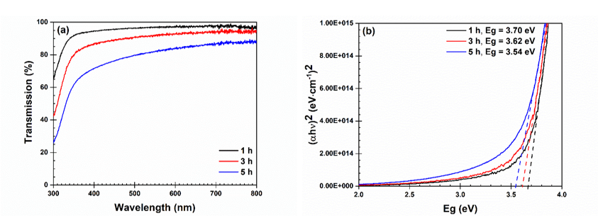
Figure 3 (a) UV-Vis transmittance spectra of TiO2 thin films at different sparking durations and (b) Corresponding Tauc plots showing optical band gap energies.
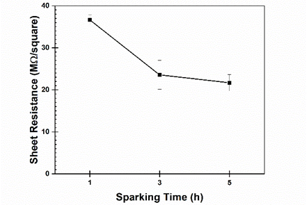
Figure 4 Sheet resistance of TiO2 thin films prepared at different sparking time of 1, 3 and 5 h.
Wetting properties of TiO2 thin films
Figure 5 illustrates the evolution of water contact angles (WCAs) for TiO2 thin films fabricated at sparking durations of 1, 3 and 5 h over an aging period of 60 days under ambient laboratory conditions. Immediately after fabrication, all samples exhibit near-superhydrophilic behavior, with initial contact angles below 5°, consistent with freshly prepared TiO2 surfaces rich in surface hydroxyl (-OH) groups and chemisorbed oxygen species [10,16]. This state is typically induced by high surface energy and the presence of oxygen vacancies that promote water dissociation and spreading [28]. However, the wettability stability varies significantly with sparking duration. After 15 - 30 days, a modest increase in WCA is observed across all samples (ranging from ~10° to ~30°), attributable to the gradual physisorption of airborne hydrocarbons and the recombination of surface-trapped electrons with lattice oxygen, which reduces -OH coverage [17]. The most striking divergence emerges after 60 days: The 1 h film retains a remarkably low contact angle of ~15°, while the 3 and 5 h films exhibit WCAs of ~110° and ~80°, respectively-indicating a transition toward hydrophobic or weakly hydrophilic states. This long-term difference can be directly correlated with surface morphology and defect structure. As shown in Figure 1, the 1 h film features a smooth, homogeneous nanostructure with fine, well-dispersed particles, which minimizes surface roughness and limits nucleation sites for hydrophobic contaminants. In contrast, prolonged sparking (3 - 5 h) yields coarse agglomerates and elevated surface roughness, which is consistent with established wetting theories, as rougher surfaces tend to amplify the intrinsic wettability state; experimentally, such rough TiO2 surfaces readily become hydrophobic upon hydrocarbon adsorption [8,9,20].
Moreover, recent studies emphasize that defect density plays a dual role: While moderate concentrations of oxygen vacancies can enhance surface hydrophilicity by increasing surface hydroxylation and water adsorption, excessive vacancies and structural disorder (as expected in thicker, thermally stressed films from longer sparking) accelerate surface recombination and increase the propensity for contamination adhesion, thus promoting hydrophobic recovery [28,13,16]. Previous studies have shown that TiO2 thin films possessing moderate grain size and low surface roughness maintain hydrophilicity more effectively over multi-week aging, consistent with our finding that surface uniformity strongly supports long-term wettability stability [10,11]. The durability pattern observed here is also consistent with studies showing that smooth, low-defect TiO2 surfaces maintain low WCAs over several weeks, whereas rougher, defect-rich films rapidly approach hydrophobic angles due to faster hydrocarbon adsorption kinetics [18,23]. Thus, the 1-h sparking condition not only yields optimal optical and electrical properties but also provides the most robust hydrophilic performance under ambient aging, making it particularly suitable for anti-fogging coatings, self-cleaning windows, and other surface-engineering applications where long-term wettability is critical [9,20].
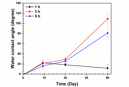
Figure 5 Variation of water contact angle on TiO2 thin films prepared at different sparking durations (1, 3 and 5 h) as a function of aging time up to 60 days.
Morphology of Au and Au-coated TiO2 thin films
Figure 6 presents SEM micrographs of pure Au thin films (Figures 6(a) - 6(c)) and Au-coated TiO2 thin films (Figures 6(d) - 6(f)) deposited under sputtering currents of 10, 30 and 50 mA. At 10 mA, both substrates exhibit discontinuous, island-like Au nanoparticles with large interparticle voids. This morphology is characteristic of the Volmer-Weber nucleation mode of noble metals on oxide and glass substrates, where weak metal-substrate interactions and high adatom mobility promote the formation of isolated 3D clusters rather than layer-by-layer growth [2,28]. The insufficient adatom flux at low sputtering current further decreases nucleation density, delaying coalescence and preventing the formation of continuous conductive pathways, consistent with early-stage growth reported for sputtered noble-metal films [6,25]. At 30 mA, the Au films become significantly more compact and continuous, with densely distributed nanoparticles forming a well-connected metallic network. This transition reflects the optimized balance between deposition flux and surface diffusion that enhances cluster coalescence and surface coverage [1,2,6]. Continuous metallic domains are known to reduce charge-transport barriers and improve optical uniformity, thereby strengthening plasmonic absorption and interfacial charge transfer in photocatalytic and optoelectronic Au-TiO2 architectures [18,20,21,23,24]. A similar trend is observed for Au sputtered onto TiO2, although TiO2-owing to its higher surface energy, presence of surface hydroxyls, and defect-mediated heterogeneous nucleation-supports slightly denser Au nucleation compared with glass [19,23,28]. At 50 mA, the high deposition flux accelerates particle growth and aggregation, generating large irregular clusters and roughened surfaces. Such behavior is consistent with flux-dominated growth regimes described by the Thornton zone model, where rapid supersaturation limits adatom surface diffusion, resulting in columnar or granular rough morphologies [2,6,28]. These rough, inhomogeneous Au domains can increase electron scattering and degrade optical uniformity, ultimately weakening plasmonic coupling and interfacial charge-transfer efficiency in Au-TiO2 systems [20,23,24,29].
The nominal Au thickness was estimated based on the system deposition rate of the DC magnetron sputtering unit (Quorum Q150RS), which delivers an approximate Au deposition rate of ~0.6 nm·s−1 under the operating conditions used in this work. Accordingly, the equivalent nominal thicknesses corresponding to sputtering currents of 10, 30 and 50 mA are ≈6, ≈18, and ≈30 nm, respectively. These values represent system-specific nominal thicknesses and reflect the expected island-growth morphology of ultrathin Au films. Due to the island-growth behavior of Volmer-Weber systems, these represent equivalent thicknesses assuming uniform coverage rather than the physical thickness of a fully continuous layer [25,28]. Nevertheless, the observed morphology aligns with the expected percolation behavior of ultrathin Au films on oxide substrates, where metallic conduction typically emerges at a nominal thickness of ~15 - 20 nm [23,25]. Overall, the comparative analysis confirms that 30 mA yields the most continuous and homogeneous Au morphology on both glass and TiO2 substrates, offering the optimal balance of electrical connectivity, optical homogeneity, and interfacial functionality for plasmonic, transparent conductive, and photocatalytic applications.
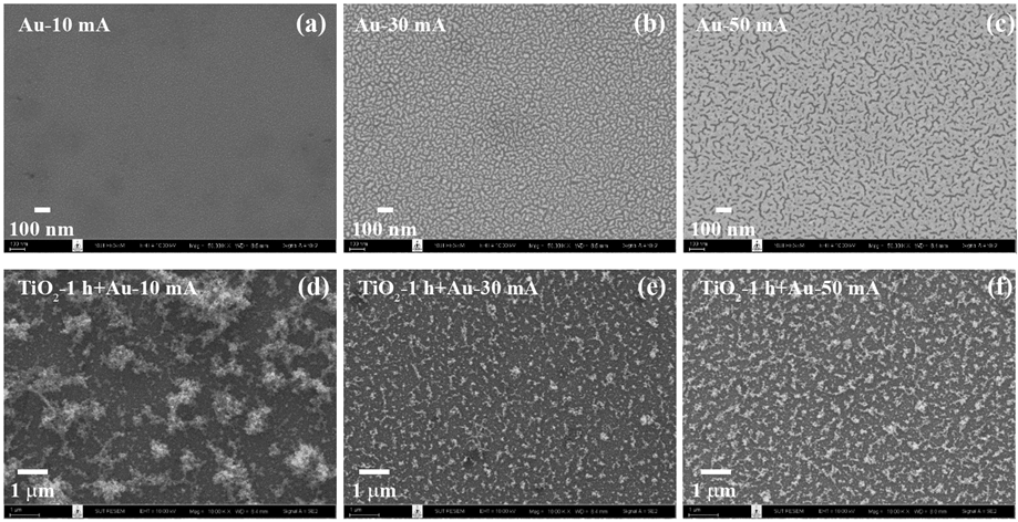
Figure 6 SEM images of Au thin films deposited on glass at (a) 10 mA, (b) 30 mA, and (c) 50 mA, and Au-coated TiO2 thin films prepared at (d) 10 mA, (e) 30 mA, and (f) 50 mA.
Compositional evolution of Au-coated TiO2 thin films with sputtering current
Energy-dispersive X-ray spectroscopy (EDS) was employed to elucidate the elemental composition of Au-coated TiO2 thin films at different sputtering currents (Table 1) [3,24,25]. A systematic increase in Au content is observed, rising from 1.40 wt.% at 10 mA to 6.60 wt.% at 30 mA and reaching 14.30 wt.% at 50 mA; these figures reflect the sample data summarized in Table 1. This monotonic trend clearly reflects the direct dependence of Au loading on the discharge current, higher currents generally enhance ion bombardment, sputtering yield, and the flux of Au atoms toward the substrate surface, consistent with experimental reports on Au deposition and coverage on TiO2 under increased deposition conditions [21,22,25] and general sputtering phenomenology (recommended to cite a sputtering-theory/review source). Oxygen remains the dominant constituent (55.1 - 65.2 wt.%) in all coated samples, consistent with the underlying TiO2 matrix being the major oxygen source [1,4,16]. Minor decreases in the oxygen fraction at higher Au loadings are interpreted as partial surface masking by Au nanoparticles rather than chemical modification of TiO2 [23,24]. Titanium is detectable primarily in Au-coated films (up to 2.7 wt.%), supporting the conclusion that Au forms a surface layer without substantial interdiffusion or alloying with the TiO2 substrate under the current deposition conditions [19,24,25]. Low-level impurities (Na, Mg, Al, Ca, K) remain below 5 wt.% and are attributed to the soda-lime glass substrate or adventitious surface contamination, a common observation for oxide films deposited on commercial glass substrates [10,11]. Notably, the TiO2-1 h + Au (50 mA) sample exhibits the highest Au concentration (15.60 wt.%), confirming efficient surface coverage at elevated sputtering currents [21,22,25].
Table 1 The percentage by weight of Element from EDS analysis.
Thin films |
Element (wt.%) |
||||||||
Au |
O |
Ti |
Na |
Mg |
Al |
Ca |
K |
Total |
|
Au 10 mA |
1.40 |
65.20 |
0.00 |
16.70 |
4.60 |
2.30 |
8.90 |
0.90 |
100.00 |
Au 30 mA |
6.60 |
60.90 |
0.00 |
16.60 |
4.70 |
2.00 |
8.70 |
0.50 |
100.00 |
Au 50 mA |
14.30 |
55.80 |
0.00 |
15.40 |
4.00 |
1.80 |
8.10 |
0.60 |
100.00 |
TiO2-1 h + Au 10 mA |
1.90 |
64.10 |
2.70 |
15.30 |
4.50 |
2.20 |
8.60 |
0.80 |
100.00 |
TiO2-1 h + Au 30 mA |
7.90 |
60.70 |
1.00 |
14.90 |
4.30 |
2.20 |
8.30 |
0.70 |
100.00 |
TiO2-1 h + Au 50 mA |
15.60 |
55.10 |
1.00 |
13.60 |
4.00 |
1.90 |
7.90 |
0.80 |
|
Plasmonic-Enhanced Sub-Band-Gap absorption in Au-coated TiO2 thin films
Figure 7(a) presents the optical transmittance spectra of Au-coated TiO2 thin films sputtered at 10, 30 and 50 mA, compared with the pristine TiO2 film (1 h sparking). All samples exhibit transparent coatings, though their transmittance decreases systematically with increasing Au loading. The pristine TiO2 film shows high transparency (~90% at 700 - 800 nm), whereas the Au-TiO2 films display reduced transmittance of ~85% (10 mA), ~70% (30 mA), and ~55% (50 mA). This monotonic decline arises from light absorption and scattering by Au nanoparticles, consistent with the localized surface plasmon resonance (LSPR) of Au in the 520 - 560 nm region, a behavior widely reported for Au-decorated TiO2 systems [1-5,14,15,36,37]. At 10 mA, Au nanoparticles remain small and sparsely distributed (Figure 6(a)), leading to minimal optical disturbance. Increasing the current to 30 mA produces a denser and more uniform Au layer (Figure 6(b)), enhancing plasmonic absorption, a trend consistent with size- and density-dependent plasmon tunability reported in Au- TiO2 nanocomposites [6-9,37,38]. At 50 mA, large Au agglomerates (Figure 6(c)) induce pronounced scattering and lower transmittance, in agreement with earlier findings on plasmonic damping and overloading effects in metal-oxide films [10-13].
Figure 7(b) reveals two distinct linear regions in the Tauc plots of all Au-coated films, characteristic of dual absorption pathways. The higher-energy onset (~3.6 - 3.9 eV) corresponds to the intrinsic inter-band transition of anatase TiO2, with slight blue-shifting attributable to nanograin-size effects. This low-energy feature does not represent a true narrowing of the intrinsic TiO2 band gap; instead, it corresponds to an effective optical absorption onset arising from the combined contributions of LSPR-induced absorption by Au nanoparticles (520 - 560 nm), metal-induced gap states (MIGS) formed at the Au-TiO2 interface, and defect-related states associated with oxygen vacancies and Ti3+ centers generated during the sputtering process. These explanations align with established mechanisms of plasmon-mediated sub-band-gap absorption in metal-modified TiO2 reported by Tian, Tatsuma, Furube, Lian, and others [1-4,16-18,39,40]. The Au-TiO2 interface forms a Schottky junction upon contact, governed by the work-function difference between Au (~5.1 eV) and n-type TiO2 (electron affinity ~4.2 eV). Electron transfer from TiO2 to Au establishes a depletion region and internal electric field that promotes electron trapping, inhibits recombination, and enhances charge separation. Extensive studies have demonstrated that Au nanoparticles can generate plasmon-induced hot electrons capable of crossing this Schottky barrier and injecting into the TiO2 conduction band, driving visible-light photoactivity [1,2,7,17,18,40,41].
Recent studies demonstrate that the interfacial electric field at the Au-TiO2 junction reduces the activation energy for hot-electron transfer, thereby shifting the effective optical absorption onset toward lower photon energies without altering the intrinsic TiO2 band structure [37,38]. This behavior is consistent with plasmon-induced charge separation and hot-electron injection processes widely reported in Au/TiO2 Schottky nanostructures [34-39]. The dual-slope behavior observed in the Tauc plots of Au-modified TiO2 films is therefore commonly attributed to the coexistence of intrinsic band-to-band transitions and additional sub-band-gap absorption channels arising from plasmon-assisted electronic transitions and defect-related states [19,21,37-38]. Such observations further indicate that the apparent band-gap narrowing in Au-TiO2 systems originates from enhanced LSPR intensity and defect-mediated absorption rather than from modifications to the crystal structure of TiO2 [10,13]. While the 50 mA sample exhibits a favorable low-energy onset (1.80 eV), its reduced transmittance (~55%) and agglomerated morphology limit applicability in transparent devices. In contrast, the 30 mA film achieves an optimal balance, providing sufficient Au coverage for strong sub-band-gap absorption (2.23 eV), moderate transparency (~70%), and uniform Au nanoparticle distribution. In comparison with previously reported plasmonic Au-TiO₂ systems, where enhanced sub-band-gap absorption is often accompanied by reduced visible transmittance at high Au loadings, the 30 mA sample in this work achieves a more favorable trade-off between visible-light absorption and optical transparency [19,21,34-39]. From a semi-quantitative perspective, this behavior can be interpreted in terms of a percolation-assisted plasmonic response, where increasing Au coverage enhances plasmon-assisted electronic transitions as the system approaches the percolation regime, leading to the observed evolution of the Tauc-plot slopes [19,21,39,40]. Such synergistic plasmonic-defect-interface effects are increasingly recognized as the primary drivers of optical modulation in noble-metal-modified oxide films [11-13,39,40].
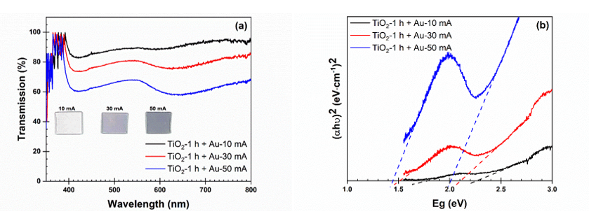
Figure 7 (a) Optical transmittance spectra of Au-coated TiO2 thin films sputtered at 10, 30 and 50 mA, with inset photographs showing the corresponding films on glass substrates; (b) Tauc plots exhibiting two distinct absorption onsets corresponding to (i) the intrinsic anatase TiO2 band-edge transition and (ii) an effective sub-band-gap absorption onset induced by Au-related plasmonic and interfacial states.
Wettability of Au-modified TiO2 thin films
Figure 8 shows the evolution of water contact angles (WCAs) of Au-coated TiO2 thin films (TiO2-1 h + Au at 10, 30 and 50 mA) over a 60-day aging period under ambient conditions. All samples exhibit low initial contact angles (~12 - 18°), confirming their inherent hydrophilicity, a well-established characteristic of TiO2 surfaces enriched with hydroxyl (-OH) groups, oxygen vacancies, and photoactivated surface states [25,26,28]. Notably, all Au-TiO2 films retain hydrophilicity throughout the entire aging period, with WCAs remaining below 30°, in contrast to the pristine 1 h TiO2 film, which, while relatively stable, still shows a gradual increase to ~15° (Figure 5). This enhanced durability strongly suggests that Au nanoparticles suppress hydrophobic recovery, a common aging effect in metal oxides caused by hydrocarbon adsorption and surface dehydroxylation [29,30]. Among the Au-coated samples, the 30 mA film demonstrates the most stable wettability, maintaining a final contact angle of only ~22° after 60 days. The 10 mA sample displays a moderate increase to ~28°, while the 50 mA film stabilizes at ~25°. This performance trend correlates closely with the nanoparticle morphology observed in SEM (Figures 6 - 8): The 30 mA coating shows a uniform, well-dispersed distribution of Au nanoparticles, maximizing interfacial contact and supporting sustained hydroxylation; the 10 mA coating exhibits insufficient Au coverage, providing limited protection against aging; and the 50 mA sample, despite higher Au loading, displays localized agglomeration that reduces effective surface energy and weakens water-solid interaction.
Recent studies align with this interpretation. Several works have shown that uniformly dispersed Au nanoparticles significantly delay hydrophobic recovery by stabilizing surface-trapped electrons and suppressing recombination with adsorbed oxygen species, mechanisms essential for maintaining surface -OH groups [31,34]. Other researchers have demonstrated that optimal (non-excessive) Au loading enhances long-term hydrophilicity by balancing plasmon-induced activation with the physical barrier function that prevents hydrocarbon adsorption [35,36]. Additional reports indicate that Au-TiO2 interfaces can regenerate hydrophilic sites under visible or ambient light, extending hydrophilicity lifetime without requiring UV excitation [37-39]. Taken together, these findings indicate that the enhanced stability of the Au-modified TiO2 films likely arises from three synergistic mechanisms: (i) electron trapping at the Au-TiO2 Schottky junction, which suppresses charge recombination and preserves reactive oxygen species; (ii) plasmonic activation under ambient illumination, which enables continuous surface cleaning and regeneration of hydroxyl groups; and (iii) physical blocking of airborne hydrocarbons by well-dispersed Au nanoparticles, minimizing contamination of active TiO2 sites [40-42]. Consequently, the 30 mA Au coating represents the optimal condition, balancing high optical transmittance, improved electrical conductivity, and exceptional long-term wettability stability, making it highly suitable for real-world applications such as self-cleaning windows, anti-fogging coatings, and biomedical surfaces, where persistent hydrophilicity under ambient conditions is essential.
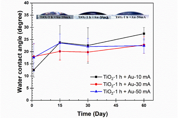
Figure 8 Water contact angles of Au-coated TiO2 thin films sputtered at 10, 30 and 50 mA, measured over 60 days, and insets show representative droplet images for each sputtering condition.
The influence of sputtering current on sheet resistance in Au-modified TiO2 thin films
The electrical behavior of TiO2 thin films changed dramatically after Au incorporation. Figure 9 shows that the pristine TiO2 film exhibits a high sheet resistance of approximately 37 MΩ/sq, characteristic of uncoated and discontinuous oxide networks [1,10]. After Au deposition, the sheet resistance decreased drastically to 7.2 Ω/sq (10 mA), 5.8 Ω/sq (30 mA), and 6.5 Ω/sq (50 mA). This six-order-of-magnitude reduction originates from the formation of metallic percolation pathways created by interconnected Au nanoparticle networks on the TiO2 surface, which enable electrons to bypass resistive TiO2 grain boundaries and migrate through low-resistance metallic bridges [19-21,36-38]. Moreover, the Au-TiO2 Schottky junctions formed at nanoparticle interfaces contribute to directional electron transport by establishing preferential pathways for charge extraction, further reducing effective sheet resistance [37,39]. Despite the overall enhancement, the dependence of conductivity on sputtering current exhibits a non-monotonic trend, reflecting the delicate balance between Au nanoparticle coverage, dispersion, and agglomeration.
At 10 mA, the surface contains sparsely distributed Au clusters, resulting in incomplete percolation and limited conduction pathways. This morphology leads to higher resistance (7.2 Ω/sq) due to insufficient nanoparticle connectivity. At 30 mA, SEM analysis confirms a dense and uniformly dispersed distribution of Au nanoparticles. This configuration provides continuous conduction paths with minimal electron-scattering barriers, achieving the lowest sheet resistance of 5.8 Ω/sq, indicative of an optimally formed percolation network. At 50 mA, the significantly higher Au flux promotes particle coalescence and cluster formation. Although the total Au content increases, the resulting larger aggregates reduce structural uniformity and disrupt long-range metallic connectivity. These agglomerated domains introduce localized barriers and enhance electron scattering, causing the sheet resistance to rise slightly to 6.5 Ω/sq, consistent with percolation theory for overloaded metallic composites [20,21,39,40]. These findings highlight that the electrical performance of Au-modified TiO2 films is governed primarily by the nanoscale architecture of the Au network rather than the intrinsic conductivity of TiO2. A sputtering current of 30 mA provides the most favorable balance between surface coverage, interparticle connectivity, and agglomeration, making it suitable for applications requiring transparent conductive behavior, plasmon-enhanced charge transport, and hybrid metal-oxide electronic interfaces [19,21,36,38,41]. Compared with existing Au-TiO2 thin films reported in the literature, where trade-offs between electrical conductivity, optical transparency, and plasmonic functionality have been observed [19,21,36-38,41], the present approach offers an improved balance among these properties with a simple sparking/sputtering fabrication route.
From a semi-quantitative perspective, the non-monotonic variation of sheet resistance with sputtering current can be interpreted in terms of a percolation-driven transport mechanism associated with Au nanoparticle coverage on the TiO2 surface [19-21]. At low sputtering current, isolated Au nanoparticles form discontinuous islands, resulting in limited conductive pathways and relatively high sheet resistance, as commonly observed for sparsely decorated Au-TiO₂ systems [19,20]. As the sputtering current increases to an intermediate regime, the surface coverage approaches a near-percolation condition, where adjacent Au islands begin to coalesce, significantly enhancing charge transport through interconnected conductive networks and Au-TiO2 interfaces [21,36-38]. Further increasing the sputtering current leads to excessive island coalescence and morphological disorder, which can introduce enhanced electron scattering at grain boundaries and Au-TiO2 junctions, thereby increasing the sheet resistance again due to aggregation-induced transport limitations [37,38]. The evolution of sheet resistance with increasing Au coverage is consistent with percolation models for metal nanoparticle films [43,44] where a conductive network forms above a critical coverage, and charge transport is governed primarily by the connectivity of metallic islands rather than the intrinsic conductivity of the oxide matrix. Experimental observations of discrete resistivity steps during the formation of Au nanoparticle networks further support this interpretation, highlighting the transition from isolated islands to a percolated conductive network [45].
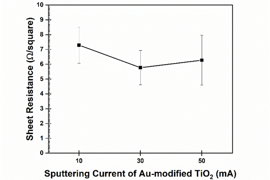
Figure 9 Sheet resistance of Au-modified TiO2 thin films as a function of sputtering current of 10, 30, and 50 mA.
Conclusions
This work demonstrates that the synergistic integration of sparking-derived TiO2 and controlled Au sputtering provides a powerful strategy for tailoring the optical, electrical, and surface-wetting characteristics of oxide thin films. The sparking duration strongly influences TiO2 microstructure, with the 1 h condition yielding the most uniform morphology, highest transparency, and best hydrophilicity retention. Subsequent Au deposition significantly enhances functional performance, but its effectiveness depends critically on nanoparticle distribution and coverage governed by the sputtering current. A sputtering current of 30 mA produces a uniformly percolated Au network that maximizes plasmonic absorption, achieves the lowest sheet resistance (5.8 Ω/sq), and stabilizes long-term hydrophilicity through both electronic and surface-barrier mechanisms. In contrast, insufficient Au loading at 10 mA and excessive agglomeration at 50 mA result in suboptimal optical and electrical behavior. Overall, the optimal TiO2-1 h + Au (30 mA) configuration offers an ideal balance of transparency, conductivity, visible-light activation, and aging resistance, making it highly suitable for transparent optoelectronics, self-cleaning coatings, and plasmon-enhanced photocatalytic applications. The findings provide clear guidelines for engineering metal-oxide thin films through simple, scalable fabrication processes. Compared with existing Au-TiO₂ thin films reported in the literature, the present approach offers an improved balance between electrical conductivity, optical transparency, and plasmonic functionality without complex fabrication steps.
Acknowledgements
This work was supported by the Faculty of Science and Technology, Nakhon Ratchasima Rajabhat University, Nakhon Ratchasima 30000, Thailand. The authors would like to thank Khajondach Viangsong for assistance with the UV-Vis spectroscopy setup and four-point probe measurements.
Declaration of Generative AI in Scientific Writing
This manuscript utilized generative AI tools, namely Qwen, ChatGPT (OpenAI), and Grammarly, which were used solely for language editing, grammar correction, and structural suggestions during the preparation of this manuscript. All scientific content, data interpretation, experimental design, and final wording decisions were made exclusively by the author. The use of AI complies with the ethical guidelines for scientific publishing. The authors affirm that they are fully responsible for the intellectual content, scientific accuracy, and integrity of this manuscript.
CRediT Author Statement
Buppachat Toboonsung: Conceptualization; Methodology; Software; Formal analysis; Resources; Writing – review & editing; Supervision; Validation; Investigation; Funding acquisition. Phinkaew Maisungnoen: Data curation; Software; Visualization; Formal analysis; Writing - Original draft preparation; Investigation; Funding acquisition.
References
[1] J Xu, H Nagasawa, M Kanezashi and T Tsuru. UV-protective TiO2 thin films with high transparency in visible light region fabricated via atmospheric-pressure plasma-enhanced chemical vapor deposition. ACS Applied Materials & Interfaces 2018; 10(49), 42657-42665.
[2] J Xu, H Nagasawa, M Kanezashi and T Tsuru. TiO2 coatings via atmospheric-pressure plasma-enhanced chemical vapor deposition for enhancing the UV-resistant properties of transparent plastics. ACS Omega 2021; 6(2), 1370-1377.
[3] SN Sadikin, J Ridwan, MIA Umar, AAM Raub, J Yunas, AA Hamzah, D Dahlan, MYA Rahman and AA Umar. Photocatalytic activity and stability properties of porous TiO2 film as photocatalyst for methylene blue and methylene orange degradation. International Journal of Electrochemical Science 2023; 18(9), 100246.
[4] A Lakshmi-Narayana, L Zhang, C Jiao, CM Julien and Y Qiu. TiO2 thin films on Au/Ti/SiO2/textured Si substrates as high capacity anode materials for Li-ion batteries. Ceramics International 2020; 46(8), 10299-10308.
[5] Y Bougdid, G Kulkarni, F Chenard, CJ Sugrim, R Kumar and A Kar. Optical properties of transparent TiO2 films by sintering anatase nanoparticles with a CO2 laser. Optical Materials 2024; 156, 115969.
[6] X Tian, X Cui, T Lai, J Ren, Z Yang, M Xiao, B Wang, X Xiao and Y Wang. Gas sensors based on TiO2 nanostructured materials for the detection of hazardous gases: A review. Nano Materials Science 2021; 3(4), 390-403.
[7] D Nunes, E Fortunato and R Martins. Flexible nanostructured TiO2-based gas and UV sensors: A review. Discover Materials 2022; 2, 2.
[8] A Nath, LR Singh and MB Sarkar. Enhanced surface wettability of Ag: TiO2 heterostructured assembly using double step glancing angle deposition technique. Ceramics International 2022; 48(8), 11392-11400.
[9] P Cai, M Xu, M Wei, T Zhang and F Yao. Preparation and characterization of SiO2-TiO2 superhydrophilic coatings with photocatalytic activity induced by low temperature. Colloids and Surfaces A: Physicochemical and Engineering Aspects 2024; 686, 133264.
[10] B Toboonsung. Electrical sheet resistance and wetting properties of TiO2 nanoparticle thin films prepared by sparking process. Advanced Materials Research 2017; 866, 313-317.
[11] B Toboonsung. Surface morphologies and durability on water contact angle of titanium dioxide nanoparticle thin films. Key Engineering Materials 2019; 798, 158-162.
[12] JA Rengifo-Herrera, P Osorio-Vargas and C Pulgarin. A critical review on N-modified TiO2 limits to treat chemical and biological contaminants in water. Evidence that enhanced visible light absorption does not lead to higher degradation rates under whole solar light. Journal of Hazardous Materials 2022; 425, 127979.
[13] YE Tasisa, TK Sarma, R Krishnaraj and S Sarma. Band gap engineering of titanium dioxide (TiO2) nanoparticles prepared via green route and its visible-light-driven application for environmental remediation. Results in Chemistry 2024; 11, 101850.
[14] J Li, Y Li, Q Lan, Z Yang and XJ Lv. Multiple phase N-doped TiO2 nanotubes/TiN/graphene nanocomposites for high-rate lithium ion batteries at low temperature. Journal of Power Sources 2019; 423, 166-173.
[15] GMV Dias, JC Bernardes, BN Wesling, D Müller, LS Marques and CR Rambo. Preparation and electrochemical capacitance of high surface area TiO2-RuO2 aerogels. Open Ceramics 2021; 8, 100196.
[16] MH Choi, CY Hong and YC Park. The hydrophilicity mechanism of anatase and rutile (110) TiO2 films based on donor-acceptor complexes. Thin Solid Films 2024; 797, 140349.
[17] J Wu and L Zhong. Predictive modeling for VOC adsorption on TiO2 filters: Implications for enhanced photocatalytic oxidation in indoor air quality management. Chemical Engineering Journal 2024; 480, 148222.
[18] J Woo, S Kim and S Lee. Durable and regenerable CuO/TiO2 coatings with long-lasting antifogging and self-cleaning abilities. Surface and Interfaces 2024; 53, 104984.
[19] KS Yang, YR Lu, YY Hsu, CJ Lin, CM Tseng, SYH Liou, K Kumar, DH Wei, CL Dong and CL Chen. Plasmon-induced visible-light photocatalytic activity of Au nanoparticle-decorated hollow mesoporous TiO2: A view by x-ray spectroscopy. Journal of Physical Chemistry C 2018; 122(12), 6955-6962.
[20] J Shondo, S Veziroglu, D Stefan, YK Mishra, T Strunskus, F Faupel and OC Aktas. Tuning wettability of TiO2 thin film by photocatalytic deposition of 3D flower- and hedgehog-like Au nano- and microstructures. Applied Surface Science 2021; 537, 147795.
[21] K Wang, K Yoshiiri, L Rosa, Z Wei, S Juodkazis, B Ohtani and E Kowalska. TiO2/Au/TiO2 plasmonic photocatalyst with enhanced photocatalytic activity and stability under visible-light irradiation. Catalysis Today 2022; 397-399, 257-264.
[22] P Birnal, MCM de Lucas, I Pochard, F Herbst, O Heintz, L Saviot, B Domenichini and L Imhoff. Visible-light photocatalytic degradation of dyes by TiO2-Au inverse opal films synthesized by atomic layer deposition. Applied Surface Science 2023; 609, 155213.
[23] AM Machinin, A Awang, CF Pien, A Samavati and A Ul-Hamid. TiO2-decorated Au nanoparticle enhances wettability of glass for self-cleaning application. Optical Materials 2023; 143, 114246.
[24] SH Han, WY Rho and BH Jun. Au-nanoparticle-embedded open-ended freestanding TiO2 nanotube arrays in dye-sensitized solar cells for better electron generation and electron transport. ACS Omega 2019; 4(23), 20346-20352.
[25] JW Gregory, Y Gong, Y Han, S Huband, RI Walton, V Hessel and EV Rebrov. Au/TiO2 coatings for photocatalytic reduction of 4-nitrophenol to 4-aminophenol with green light. Catalysis Today 2023; 418, 114145.
[26] W Thongsuwan, T Kumpika and P Singjai. Effect of high roughness on a long aging time of superhydrophilic TiO2 nanoparticle thin films. Current Applied Physics 2011; 11(5), 1237-1242.
[27] N Sharma, H Ma, T Bottein, M Bugnet, F Vocanson, D Grosso, TE Itina, Y Ouerdane and N Destouches. Crystal growth in mesoporous TiO2 optical thin films. Journal of Physical Chemistry C 2019; 123(10), 6070-6079.
[28] DNG Krishna, RP George and J Philip. Role of oxygen vacancy formation energy and insulating behavior in darkening of white amorphous TiO2. Journal of Physical Chemistry C 2021; 125(29), 16136-16146.
[29] S Sahoo, AK Arora and V Sridharan. Raman line shapes of optical phonons of different symmetries in anatase TiO₂ nanocrystals. Journal of Physical Chemistry C 2009; 113(39), 16927-16933.
[30] IA Alhomoudi and G Newaz. Residual stresses and Raman shift relation in anatase TiO2 thin film. Thin Solid Films 2009; 517(15), 4372-4378.
[31] TS Senthil, N Muthukumarasamy, S Agilan, M Thambidurai and R Balasundaraprabhu. Preparation and characterization of nanocrystalline TiO2 thin films. Materials Science and Engineering B 2010; 174(1-3), 102-104.
[32] B Endrődi, E Kecsenovity, K Rajeshwar and C Janáky. One-step electrodeposition of nanocrystalline TiO2 films with enhanced photoelectrochemical performance and charge storage. ACS Applied Energy Materials 2018; 1(2), 851-858.
[33] MH Younus, GG Ali and HA Salih. The reinforced optical fiber sensing with bilayer AuNPs/SiC for pressure measurement: Characterization and optimization. Journal of Physics: Conference Series 2021; 1795, 012002.
[34] AA Jabber and AR Abdulridha. Preparation and characterization of CuO/ZnO nanostructures thin films using thermal evaporation for advanced gas sensing applications. Trends in Sciences 2025; 22(3), 9002.
[35] T Chanthong, W Intaratat and TN Wichean. Effect of thickness on electrical and optical properties of ZnO:Al films. Trends in Sciences 2023; 20(3), 6372.
[36] Y Tian and T Tatsuma. Mechanisms and applications of plasmon-induced charge separation at TiO₂ films loaded with gold nanoparticles. Journal of the American Chemical Society 2005; 127(20), 7632-7637.
[37] L Du, A Furube, K Yamamoto, K Hara, R Katoh and M Tachiya. Plasmon-induced charge separation and recombination dynamics in gold-TiO2 nanoparticle systems: Dependence on TiO2 particle size. Journal of Physical Chemistry C 2009; 113(16), 6454-6462.
[38] A Furube, L Du, K Hara, R Katoh and M Tachiya. Ultrafast plasmon-induced electron transfer from gold nanodots into TiO2 nanoparticle. Journal of the American Chemical Society 2007; 129(48), 14852-14853.
[39] N Ghorai, Z Yang, ST Gebre, S Wu, F Zhao, IN Ivanov and T Lian. Efficient size-dependent hot electron transfer from Au to TiO2 nanoparticles. Nano Letters 2025; 25(8), 3253-3258.
[40] Y Liu, Q Chen, DA Cullen, Z Xie and T Lian. Efficient hot electron transfer from small Au nanoparticles. Nano Letters 2020; 20(6), 4322-4329.
[41] DC Ratchford, AD Dunkelberger, I Vurgaftman, JC Owrutsky and PE Pehrsson. Quantification of efficient plasmonic hot-electron injection in gold nanoparticle-TiO2 films. Nano Letters 2017; 17(10), 6047-6055.
[42] VM Kaganer, B Jenichen, R Shayduk, W Braun and H Riechert. Kinetic optimum of Volmer-weber growth. Physical Review Letters 2009; 102, 016103.
[43] XM Tao, GX Ye, QL Ye, JS Jin, YF Lao and ZK Jiao. Anomalous electrical conductivity of a gold thin film percolation system. Physical Review B 2002; 66, 115406.
[44] KH Müller, J Herrmann, B Raguse, G Baxter and T Reda. Percolation model for electron conduction in films of metal nanoparticles linked by organic molecules. Physical Review B 2002; 66, 075417.
[45] MJ Lefferts, K Murugappan, C Wu, MR Castell. Electrical percolation through a discontinuous Au nanoparticle film. Applied Physics Letters 2018; 112(25), 251602.